Printed Circuit Board (PCB) design is the process of planning and creating the layout of electronic circuits on a board made of insulating material, usually fiberglass or polyimide. Conductive copper tracks are etched onto the surface to interconnect components such as resistors, capacitors, ICs, and connectors.
PCBs are the foundation of all modern electronics — from simple calculators to aerospace systems — as they ensure compactness, reliability, and ease of manufacturing.
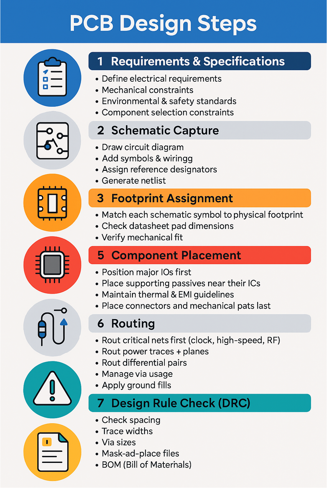
Steps in PCB Design
Requirement Analysis
- Define circuit purpose, performance, and size constraints
Schematic Capture
- Draw the circuit diagram in design software (e.g., KiCad, Altium, Eagle, OrCAD)
- Assign connections between components
Component Selection & Footprints
- Choose parts considering cost, availability, and specifications
- Assign footprints (pad layouts) to match actual components
Board Outline & Layer Setup
- Define the board shape and number of layers (single, double, or multilayer)
Component Placement
- Place parts logically (inputs, processors, outputs)
- Keep heat-generating components apart
- Optimize placement for routing and manufacturing
Routing
- Connect components with copper traces
- Control trace width, spacing, and impedance
- Separate analog, digital, and power paths to avoid noise
Design Rule Check (DRC)
- Run automated checks for spacing, clearance, and connectivity errors
Simulation & Verification
- Check signal integrity, EMI/EMC compliance, and power delivery
Gerber File Generation
- Export final files for fabrication (Gerber, drill, pick-and-place)
Types of PCB
• Single-layer PCB: Simple, low-cost
• Double-layer PCB: More routing options
• Multilayer PCB: High density, used in complex systems
• Rigid PCB: Standard boards
• Flexible PCB (FPCB): Bendable for compact devices
• Rigid-Flex PCB: Hybrid for advanced electronics
PCB Layout Guide
PCB (Printed Circuit Board) Layout is the process of designing the physical arrangement of components and electrical connections on a PCB. The layout is critical as it directly affects functionality, reliability, and manufacturability.
Importance of PCB Layout
- Signal Integrity: Proper layout reduces noise, crosstalk, and electromagnetic interference (EMI)
- Thermal Management: Efficient placement of components ensures proper heat dissipation
- Power Efficiency: Shorter traces for high-current paths reduce voltage drops
- Manufacturability: Well-designed layouts simplify assembly and testing